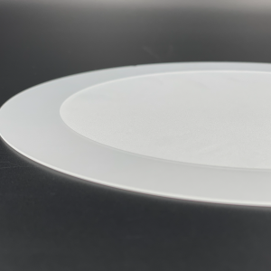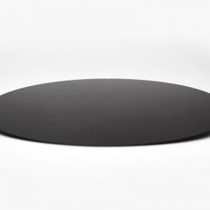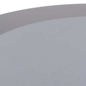
Carrier wafers are used for thin wafer handling by supporting the device wafer with a rigid carrier during processing. Wafer Universe carriers are reusable for many temporary bonds. Those carriers made of Borofloat33® glass and SCG72 are perfectly adapted to Silicon and GaAs device wafers due to their similar coefficient of thermal expansion (cte). Carriers from black quartz enable automatic loading of wafers by common wafer handling systems (IR-controlled) caused by their black opacity and IR blockage. This unique material offers various advantages for semiconductor applications due to similar properties as fused silica. Adapter Carrier Wafers enables the processing of wafers with various diameters on the same tool. The carrier diameter fits to your processing equipment and allows processing of different wafer diameter without need of expensive equipment change or tool implementation. Adapter carriers enable the processing of wafers with various diameters on the same tool. The carrier diameter fits your processing equipment and allows processing of different wafer diameters without needing an expensive equipment change or tool implementation. Due to non-conductive material properties whilst avoiding alkaline ions, these carriers are suitable for tasks which do not allow conductive materials.