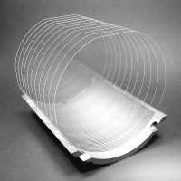
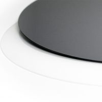
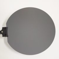
Glass wafers made of Borofloat33® glass are often used in Semiconductor and MEMS industry in a wide variety of applications. These wafers can be used for the encapsulation of MEMS devices for example for sensors using Wafer-Level-Packaging (WLP) technology or as blank glass substrates for semiconductor processing and optics.
Wafer Universe stock products from Borofloat33® glass have a coefficient of thermal expansion (cte) that is adapted to silicon, which makes them the perfect substrate to use in anodic bonding. The glass features good transmission over a wide spectrum as well as high chemical resistance and mechanical strength. Furthermore, these wafers can be used in high temperature processing.

