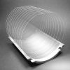
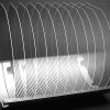
Glass wafers made of Borofloat33® glass are often used in Semiconductor and MEMS industry in a wide variety of applications. These wafers can be used for the encapsulation of MEMS devices for example for sensors using Wafer-Level-Packaging (WLP) technology or as blank glass substrates for semiconductor processing and optics.
Wafer Universe stock products from Borofloat33® glass have a coefficient of thermal expansion (cte) that is adapted to silicon, which makes them the perfect substrate to use in anodic bonding. The glass features good transmission over a wide spectrum as well as high chemical resistance and mechanical strength. Furthermore, these wafers can be used in high temperature processing.
100 mm wafers
- material: Borofloat33® glass
- cte: 3.25 ppm/K (adapted to Si)
- diameter: 100 mm
- diameter tolerance: ± 0.3 mm
- thickness tolerance: ± 10 μm
- polishing: double side polished
- surface roughness (Ra): < 1 nm
- ttv: < 10 μm
- bow: < 30 μm
- flat: according to SEMI (32.5 mm)
- surface: scratch-dig 60-40 according MIL-PRF-13830
- edge exclusion: 6 mm
- packing: clean room packed under ISO 6 conditions according to ISO 14644
- packing units: 10 pcs, 25 pcs
- material data sheet
150 mm wafers
- material: Borofloat33® glass
- cte: 3.25 ppm/K (adapted to Si)
- diameter: 150 mm
- diameter tolerance: ± 0.3 mm
- thickness tolerance: ± 10 μm
- polishing: double side polished
- surface roughness (Ra): < 1 nm
- ttv: < 10 μm
- bow: < 60 μm
- flat: according to SEMI (57.5 mm)
- surface: scratch-dig 60-40 according MIL-PRF-13830
- edge exclusion: 6 mm
- packing: clean room packed under ISO 6 conditions according to ISO 14644
- packing units: 10 pcs, 25 pcs
- material data sheet
200 mm wafers
- material: Borofloat33® glass
- cte: 3.25 ppm/K (adapted to Si)
- diameter: 200 mm
- diameter tolerance: ± 0.3 mm
- thickness tolerance: ± 10 μm
- polishing: double side polished
- surface roughness (Ra): < 1 nm
- ttv: < 10 μm
- bow: < 80 μm
- notch: according to SEMI
- surface: scratch-dig 60-40 according MIL-PRF-13830
- edge exclusion: 6 mm
- packing: clean room packed under ISO 6 conditions according to ISO 14644
- packing units: 10 pcs, 25 pcs
- material data sheet
300 mm wafers
- material: Borofloat33® glass
- cte: 3.25 ppm/K (adapted to Si)
- diameter: 300 mm
- diameter tolerance: ± 0.3 mm
- thickness tolerance: ± 10 μm
- polishing: double side polished
- surface roughness (Ra): < 1 nm
- ttv: < 10 μm
- bow: < 100 μm
- notch: according to SEMI
- surface: scratch-dig 60-40 according MIL-PRF-13830
- edge exclusion: 6 mm
- packing: clean room packed under ISO 6 conditions according to ISO 14644
- packing units: 10 pcs, 25 pcs
- material data sheet
Additional products
BOROFLOAT33® GLASS WAFERS
WITH MDF POLISHING GRADE
ALKALINE FREE GLASS WAFERS
QUARTZ WAFERS
SEMICONDUCTOR GRADE
QUARTZ WAFERS
HP FUSED SILICA
CARRIER WAFER
FOR LASER / MECHANICAL RELEASE
BLACK QUARTZ CARRIER
SI-ADAPTER CARRIER
GLASS-ADAPTER CARRIER
Ask for quotation!
Have you found a suitable product? Contact us now for an individual offer.

