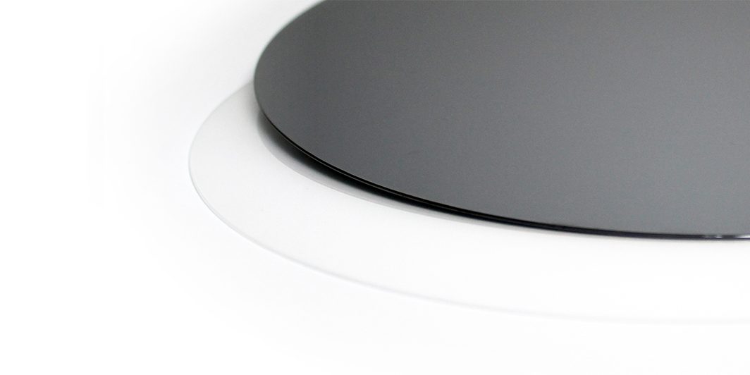
Due to their low thickness, semiconductor wafers are vulnerable to stress and breakage. Warping of the wafers during handling and processing causes a high yield loss or even makes it impossible to handle the wafers any more. This means, a Thin wafer handling technology with a high grade of flexibility on wafer and substrate sizes is needed.
Plan Optik is producing carriers for thin wafer handling with a high expertise since many years. Due to an increased demand for fastidious carriers available in short lead times, Wafer Universe is now providing such carriers with common specifications off the shelf. Those carriers are specially made for laser and mechanical de-bonding processes.
Coefficient of thermal expansion (cte) of the used materials is adapted to silicon or gallium arsenide. Different grades of ttv (down to < 1µm) and thickness tolerances (down to ±3 µm) enable a smoothly integration in running productions. All carriers are available for various wafer diameters (150mm, 200mm, 300mm) off the shelf with a lead time of less than one week. -> See our new carrier wafers!


